Q1. When negative voltage feedback is applied to an amplifier, its voltage gain ……………….
- Is increased
- Is reduced
- Remains the same
- None of the above
Answer : 2
Q2. The value of negative feedback fraction is always …………….
- Less than 1
- More than 1
- Equal to 1
- None of the above
Answer : 1
Q3. If the output of an amplifier is 10 V and 100 mV from the output is fed back to the input, then feedback fraction is ………..
- 10
- 1
- 01
- 15
Answer : 3
Q4. The gain of an amplifier without feedback is 100 db. If a negative feedback of 3 db is applied, the gain of the amplifier will become …………..
- 5 db
- 300 db
- 103 db
- 97 db
Answer : 4
Q5. If the feedback fraction of an amplifier is 0.01, then voltage gain with negative feedback is approximately………..
- 500
- 100
- 1000
- 5000
Answer : 2
Q6. A feedback circuit usually employs ……………… network
- Resistive
- Capacitive
- Inductive
- None of the above
Answer : 1
Q7. The gain of an amplifier with feedback is known as ………….. gain
- Resonant
- Open loop
- Closed loop
- None of the above
Answer : 3
Q8. When voltage feedback (negative) is applied to an amplifier, its input impedance ………….
- Is decreased
- Is increased
- Remains the same
- None of the above
Answer : 2
Q9. When current feedback (negative) is applied to an amplifier, its input impedance …………..
- Is decreased
- Is increased
- Remains the same
- None of the above
Answer : 1
Q10. Negative feedback is employed in ……………..
- Oscillators
- Rectifiers
- Amplifiers
- None of the above
Answer : 3
Q11. Emitter follower is used for …………
- Current gain
- Impedance matching
- Voltage gain
- None of the above
Answer : 2
Q12. The voltage gain of an emitter follower is ………..
- Much less than 1
- Approximately equal to 1
- Greater than 1
- None of the above
Answer : 2
Q13. When current feedback (negative) is applied to an amplifier, its output impedance ……..
- Is increased
- Is decreased
- Remains the same
- None of the above
Answer : 1
Q14. Emitter follower is a ……………….. circuit
- Voltage feedback
- Current feedback
- Both voltage and current feedback
- None of the above
Answer : 2
Q15. If voltage feedback (negative) is applied to an amplifier, its output impedance …………..
- Remains the same
- Is increased
- Is decreased
- None of the above
Answer : 3
Q16. When a negative voltage feedback is applied to an amplifier, its bandwidth……….
- Is increased
- Is decreased
- Remains the same
- Insufficient data
Answer : 1
Q17. An emitter follower has ………… input impedance
- Zero
- Low
- High
- None of the above
Answer : 3
Q19. The output impedance of an emitter follower is ……….
- High
- Very high
- Almost zero
- Low
Answer : 4
Q1. An oscillator converts ……………..
- c. power into d.c. power
- c. power into a.c. power
- mechanical power into a.c. power
- none of the above
Answer : 2
Q2. In an LC transistor oscillator, the active device is ……………
- LC tank circuit
- Biasing circuit
- Transistor
- None of the above
Answer : 3
Q3. In an LC circuit, when the capacitor is maximum, the inductor energy is ……….
- Minimum
- Maximum
- Half-way between maximum and minimum
- None of the above
Answer : 1
Q4. In an LC oscillator, the frequency of oscillator is ……………. L or C.
- Proportional to square of
- Directly proportional to
- Independent of the values of
- Inversely proportional to square root of
Answer : 4
Q5. An oscillator produces……………. oscillations
- Damped
- Undamped
- Modulated
- None of the above
Answer : 2
Q6. An oscillator employs ……………… feedback
- Positive
- Negative
- Neither positive nor negative
- Data insufficient
Answer : 1
Q7. An LC oscillator cannot be used to produce ……………….. frequencies
- High
- Audio
- Very low
- Very high
Answer : 3
Q8. Hartley oscillator is commonly used in ………………
- Radio receivers
- Radio transmitters
- TV receivers
- None of the above
Answer : 1
Q9. In a phase shift oscillator, we use …………. RC sections
- Two
- Three
- Four
- None of the above
Answer : 2
Q10. In a phase shift oscillator, the frequency determining elements are …………
- L and C
- R, L and C
- R and C
- None of the above
Answer : 3
Q11. A Wien bridge oscillator uses ……………. feedback
- Only positive
- Only negative
- Both positive and negative
- None of the above
Answer : 3
Q12. The piezoelectric effect in a crystal is ……………
- A voltage developed because of mechanical stress
- A change in resistance because of temperature
- A change in frequency because of temperature
- None of the above
Answer : 1
Q13. If the crystal frequency changes with temperature, we say that crystal has ………….. temperature coefficient
- Positive
- Zero
- Negative
- None of the above
Answer : 1
Q14. The crystal oscillator frequency is very stable due to ………………. of the crystal
- Rigidity
- Vibrations
- Low Q
- High Q
Answer : 4
Q15. The application where one would most likely find a crystal oscillator is ……………..
- Radio receiver
- Radio transmitter
- AF sweep generator
- None of the above
Answer : 2
Q16. An oscillator differs from an amplifier because it ………
- Has more gain
- Requires no input signal
- Requires no d.c. supply
- Always has the same input
Answer : 2
Q17. One condition for oscillation is ………….
- A phase shift around the feedback loop of 180o
- A gain around the feedback loop of one-third
- A phase shift around the feedback loop of 0o
- A gain around the feedback loop of less than 1
Answer : 3
Q18. A second condition for oscillations is ……………….
- A gain of 1 around the feedback loop
- No gain around the feedback loop
- The attention of the feedback circuit must be one-third
- The feedback circuit must be capacitive
Answer : 1
Q19. In a certain oscillator Av = 50. The attention of the feedback circuit must be …………
- 1
- 01
- 10
- 02
Answer : 4
Q20. For an oscillator to properly start, the gain around the feedback loop must initially be
- 1
- Greater than 1
- Less than 1
- Equal to attenuation of feedback circuit
Answer : 2
Q21. In a Wien-bridge oscillator, if the resistances in the positive feedback circuit are decreased, the frequency……….
- Remains the same
- Decreases
- Increases
- Insufficient data
Answer : 3
Q22. In Colpitt’s oscillator, feedback is obtained …………….
- By magnetic induction
- By a tickler coil
- From the centre of split capacitors
- None of the above
Answer : 3
Q23. The Q of the crystal is of the order of …………
- 100
- 1000
- 50
- More than 10,000
Answer : 4
Q24. Quartz crystal is most commonly used in crystal oscillators because ………….
- It has superior electrical properties
- It is easily available
- It is quite inexpensive
- None of the above
Answer : 1
Q27. ………….. is a fixed frequency oscillator
- Phase-shift oscillator
- Hartely-oscillator
- Colpitt’s oscillator
- Crystal oscillator
Answer : 4
Q28. In an LC oscillator, if the value of L is increased four times, the frequency of oscillations is …………
- Increased 2 times
- Decreased 4 times
- Increased 4 times
- Decreased 2 times
Answer : 4
Q29. An important limitation of a crystal oscillator is ……………
- Its low output
- Its high Q
- Less availability of quartz crystal
- Its high output
Answer : 1
Q30. The signal generator generally used in the laboratories is ………….. oscillator
- Wien-bridge
- Hartely
- Crystal
- Phase shift
Answer : 1
1) What are the consequences over the non-linear distortion by the inception of negative feedback?
b. Level of non-linear distortion goes on decreasing c. Level of non-linear distortion undergoes stability d. None of the above
| |||||||||||||||||||||||||||||||||||||||||||||||||||||||||||||||||||||||||||||||||||||||||||||||||||||||||||||||||||||||||||||||||||||||||||||||||||||||||||||||||||||||||||||||||||||||||||||||||||||||||||||||||||||||||||||||||||||||||||||||||||||||||||||||||||||||||||||||||||||||||||||||||||||||||||||||||||||||||||||||||||||||||||||||||||||||||||||||||||||||||||||||||||||||||||||||||||||||||||||||||||||||||||||||||||||||||||||||||||||||||||||||||||||||||||||||||||||||||||||||||||||||||||||||||||||||||||||||||||||||||||||||||||||||||||||||||||||||||||||||||||||||||||||||||||||||||||||||||
2) Stability of a transfer gain is generally defined as the reciprocal of _______
b. Conductivity c. Sensitivity d. Desensitivity
| |||||||||||||||||||||||||||||||||||||||||||||||||||||||||||||||||||||||||||||||||||||||||||||||||||||||||||||||||||||||||||||||||||||||||||||||||||||||||||||||||||||||||||||||||||||||||||||||||||||||||||||||||||||||||||||||||||||||||||||||||||||||||||||||||||||||||||||||||||||||||||||||||||||||||||||||||||||||||||||||||||||||||||||||||||||||||||||||||||||||||||||||||||||||||||||||||||||||||||||||||||||||||||||||||||||||||||||||||||||||||||||||||||||||||||||||||||||||||||||||||||||||||||||||||||||||||||||||||||||||||||||||||||||||||||||||||||||||||||||||||||||||||||||||||||||||||||||||||
3) What would happen, if the signal Xd passes through the feedback network?
b. Xd will get multiplied by 'β' c. Xd will get multiplied by '1 – Aβ' d. Xd will get multiplied by '1 + Aβ'
| |||||||||||||||||||||||||||||||||||||||||||||||||||||||||||||||||||||||||||||||||||||||||||||||||||||||||||||||||||||||||||||||||||||||||||||||||||||||||||||||||||||||||||||||||||||||||||||||||||||||||||||||||||||||||||||||||||||||||||||||||||||||||||||||||||||||||||||||||||||||||||||||||||||||||||||||||||||||||||||||||||||||||||||||||||||||||||||||||||||||||||||||||||||||||||||||||||||||||||||||||||||||||||||||||||||||||||||||||||||||||||||||||||||||||||||||||||||||||||||||||||||||||||||||||||||||||||||||||||||||||||||||||||||||||||||||||||||||||||||||||||||||||||||||||||||||||||||||||
4) After passing through which circuit/network ,does the signal Xd (output signal obtained by taking the difference of two input signals) get multiplied by '-1'?
b. Feedback network c. Mixing network d. Sampling network
| |||||||||||||||||||||||||||||||||||||||||||||||||||||||||||||||||||||||||||||||||||||||||||||||||||||||||||||||||||||||||||||||||||||||||||||||||||||||||||||||||||||||||||||||||||||||||||||||||||||||||||||||||||||||||||||||||||||||||||||||||||||||||||||||||||||||||||||||||||||||||||||||||||||||||||||||||||||||||||||||||||||||||||||||||||||||||||||||||||||||||||||||||||||||||||||||||||||||||||||||||||||||||||||||||||||||||||||||||||||||||||||||||||||||||||||||||||||||||||||||||||||||||||||||||||||||||||||||||||||||||||||||||||||||||||||||||||||||||||||||||||||||||||||||||||||||||||||||||
5) What would be the computational value of feedback voltage in a negative feedback amplifier with A = 100, β = 0.03 and input signal voltage = 30 mV?
b. 0.06 V c. 0.09 V d. 0.15 V
| |||||||||||||||||||||||||||||||||||||||||||||||||||||||||||||||||||||||||||||||||||||||||||||||||||||||||||||||||||||||||||||||||||||||||||||||||||||||||||||||||||||||||||||||||||||||||||||||||||||||||||||||||||||||||||||||||||||||||||||||||||||||||||||||||||||||||||||||||||||||||||||||||||||||||||||||||||||||||||||||||||||||||||||||||||||||||||||||||||||||||||||||||||||||||||||||||||||||||||||||||||||||||||||||||||||||||||||||||||||||||||||||||||||||||||||||||||||||||||||||||||||||||||||||||||||||||||||||||||||||||||||||||||||||||||||||||||||||||||||||||||||||||||||||||||||||||||||||||
6) Which among the following is an output provided by transresistance amplifier?
b. Output voltage proportional to signal current c. Output voltage proportional to input voltage d. Output current proportional to signal current
| |||||||||||||||||||||||||||||||||||||||||||||||||||||||||||||||||||||||||||||||||||||||||||||||||||||||||||||||||||||||||||||||||||||||||||||||||||||||||||||||||||||||||||||||||||||||||||||||||||||||||||||||||||||||||||||||||||||||||||||||||||||||||||||||||||||||||||||||||||||||||||||||||||||||||||||||||||||||||||||||||||||||||||||||||||||||||||||||||||||||||||||||||||||||||||||||||||||||||||||||||||||||||||||||||||||||||||||||||||||||||||||||||||||||||||||||||||||||||||||||||||||||||||||||||||||||||||||||||||||||||||||||||||||||||||||||||||||||||||||||||||||||||||||||||||||||||||||||||
7) Which among the below specified conditions is responsible to drive a low resistance load by the current amplifier circuit?
b. R0 >> RL c. Rs << Ri d. R0 << RL
| |||||||||||||||||||||||||||||||||||||||||||||||||||||||||||||||||||||||||||||||||||||||||||||||||||||||||||||||||||||||||||||||||||||||||||||||||||||||||||||||||||||||||||||||||||||||||||||||||||||||||||||||||||||||||||||||||||||||||||||||||||||||||||||||||||||||||||||||||||||||||||||||||||||||||||||||||||||||||||||||||||||||||||||||||||||||||||||||||||||||||||||||||||||||||||||||||||||||||||||||||||||||||||||||||||||||||||||||||||||||||||||||||||||||||||||||||||||||||||||||||||||||||||||||||||||||||||||||||||||||||||||||||||||||||||||||||||||||||||||||||||||||||||||||||||||||||||||||||
8) What should be the value of input resistance for an ideal voltage amplifier circuit?
b. Unity c. Infinity d. Unpredictable
| |||||||||||||||||||||||||||||||||||||||||||||||||||||||||||||||||||||||||||||||||||||||||||||||||||||||||||||||||||||||||||||||||||||||||||||||||||||||||||||||||||||||||||||||||||||||||||||||||||||||||||||||||||||||||||||||||||||||||||||||||||||||||||||||||||||||||||||||||||||||||||||||||||||||||||||||||||||||||||||||||||||||||||||||||||||||||||||||||||||||||||||||||||||||||||||||||||||||||||||||||||||||||||||||||||||||||||||||||||||||||||||||||||||||||||||||||||||||||||||||||||||||||||||||||||||||||||||||||||||||||||||||||||||||||||||||||||||||||||||||||||||||||||||||||||||||||||||||||
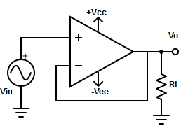
1. Voltage shunt feedback amplifier forms
a) A negative feedback b) A positive feedback c) Both positive and negative d) None of the mentioned View Answer
Answer: a
Explanation: A voltage shunt feedback amplifier forms a negative feedback because, any increase in the output signal results in a feedback signal into the inverting input causing a decrease in the output signal.
2. The value of feedback resistor and resistor connected in series with the input signal source are equal to 10kΩ and 3.3kΩ. Calculate the closed loop voltage gain?
a) -6.7 b) -33 c) -13.3 d) -3.33 View Answer
Answer: d
Explanation: Closed loop voltage gain, AF = -RF/R1 = -10kΩ/3.3kΩ = -3.33.
3. Write the formula for closed loop voltage gain of inverting amplifier with feedback using open loop voltage gain and gain of feedback circuit.
a) AF= A/(1+AB) b) AF= -A/(1+AB) c) AF= -B/(1+AB) d) None of the mentioned View Answer
Answer: c
Explanation: The closed loop voltage gain of the amplifier is AF= -Ak/(1+AB), where k is a voltage attenuation factor. In addition to phase inversion, AF is k times the closed loop gain of the non-inverting amplifier where k<1.
4. Voltage shunt feedback amplifiers are also called as
a) Non-inverting amplifier with feedback b) Non-inverting amplifier without feedback c) Inverting amplifier with feedback d) Inverting amplifier without feedback View Answer
Answer: c
Explanation: The input and output signal in voltage series feedback amplifier are 180o out of phase (or of opposite polarities). Due to this phase inversion, the configuration is also called as inverting amplifier with feedback.
5. Find the block diagram representation for inverting amplifier with feedback
 View Answer
Answer: b
Explanation: The block diagram of non-inverting amplifier is identical to that of inverting amplifier except for the voltage attenuation factor or block. However, the major difference is that a voltage summing junction is being used as a model for what is actually a current summing.
6. The inverting input inverting of the voltage shunt feedback resistor is a commonly named as
a) Terminal ground b) Virtual ground c) Virtual input d) Resistive input View Answer
Answer: b
Explanation: Ideally, the difference between input voltages is zero. Therefore, the voltage at the inverting terminal is approximately equal to that of non-inverting terminal. In other words, the inverting terminal voltage is approximately at ground potential and it is said to be virtual ground.
7. Compute RIF for an inverting amplifier with feedback, where the value of input resistance of op-amp is 4.7kΩ.
a) 4.7kΩ b) 9.4kΩ c) 2.35kΩ d) Data given is insufficient View Answer
Answer: a
Explanation: In voltage shunt feedback amplifier, the input resistance with feedback is given as RIF = R1 (ideally).
8. Specification of op-amp 741c is given below:
A=200000; Ri=2MΩ; Ro=75Ω; Supply voltages= ±15v; output voltage swing =±13v; fo=5hz. 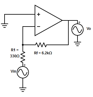 Compute the value of output resistance, bandwidth and closed loop voltage gain for the circuit shown. a) ROF=8.6mΩ , fF= 53005hz and AF=-9.36 b) ROF=4.12mΩ , fF= 53005hz and AF=-11.78 c) ROF=7.1mΩ , fF = 53005hz and AF=-16.95 d) ROF=1.9mΩ , fF= 53005hz and AF=-10 View Answer
Answer: c
Explanation: Output resistance of the amplifier, ROF= Ro/(1+AB) =, where B= R1+RF = 330Ω/330Ω+6.2kΩ = 0.053. => ROF= ±75/(1+200000*0.053) = 53005hz. Closed loop voltage gain, AF= -(A*K)/(1+AB), Where k= RF/(R1+F) = 6.2kΩ/(330Ω+6.2kΩ) = 0.949 => AF = -(200000*0.949)/[1+(200000*0.0535)] = -16.95.
9. What is the break frequency of the op-amp?
a) fo = Unity Gain Bandwidth /closed loop voltage gain b) fo = Unity Gain Bandwidth / open loop voltage gain c) fo = Unity Gain Bandwidth /Gain of feedback circuit d) All of the mentioned View Answer
Answer: c
Explanation: The mentioned formula is the general break frequency of any operational amplifier.
10. The total voltage offset voltage with feedback (VooT) equation for inverting amplifier is
a) Same as that of non-inverting amplifier b) k times the non-inverting amplifier, k-> voltage attenuation factor c) Twice the equation of non-inverting amplifier d) All of the mentioned View Answer
Answer: a
Explanation: Voot equation for inverting amplifier is the same as that of the non-inverting amplifier because, when the input signal is reduced to zero, both inverting and non-inverting amplifier results in the same circuit.
11. Which among the following is not a special case of voltage shut feedback amplifier?
a) Voltage follower b) Current to voltage connector c) Inverter d) None of the mentioned View Answer
Answer: a
Explanation: A voltage follower is a special case of non-inverting amplifier ( or voltage series feedback amplifier) and it has a gain of unity.
12. Compute the output voltage for the given circuit
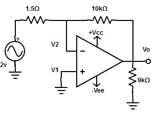 a) -2.6v b) -27.8v c) -26.7v d) -0.267v View Answer
Answer: c
Explanation: The given circuit is a current to voltage converter. Since V1 =0v and V1= V2. => iin = Vin/R1 = 4/ 1.5kΩ =2.67mA. The output voltage Vo = -iin*RF = -2.67mA*10kΩ = -26.7v.
13. At what condition an inverting amplifier works as an inverter
 a) R1 = RF+ RL b) RF =( R1*Vin)/RL c) R1 = RF d) R1 = Vo/(Vin*RL) View Answer
Answer: c
Explanation: If R1 = RF, the inverting amplifier will work as an inverter.
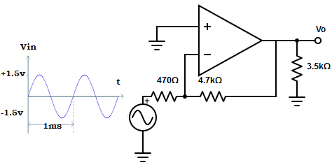
14. Determine the output waveform for the given input signal
  View Answer
Answer: a
9) Which among the following parameter/s increase/s due to positive feedback?Explanation: Given, Vin= 3Vpp sinewave at 1khz (Therefore F=1/T=1/ms =1khz) => iin= Vin/R1 = 3/ 470=6.4mA => Vo=- iin*RF=6.4mA*4.7kΩ = 30 Vpp sinewave at 1khz
1. Find the input and output resistance for the circuit shown.
Specification for 741 op-amp : A=400000 ; Ri = 33MΩ; Ro = 60Ω; RF = 11kΩ; R1 = 2kΩ; Supply voltage = ± 15v; Maximum output voltage swing = ± 13v. 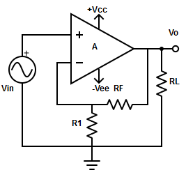 a) RIF = 66MΩ, ROF = 30Ω b) RIF = 30MΩ, ROF = 6kΩ c) RIF = 15kΩ, ROF = 50MΩ d) None of the mentioned View Answer
Answer: a
Explanation: AF = 1+(RF/R1) = 1+(11kΩ/2kΩ) = 6.5; B= 1/ AF = 1/6.5 = 0.154; Input resistance of RIF = R1(1+AB) = 33MΩ[1+(6.5*0.154) ]= 66MΩ; Output resistance of ROF = Ro/(1+AB) = 60/[1+(6.5*0.154) ]= 29.98 ≅30Ω.
2. The output resistance of the op-amp with feedback is
a) Same as that of the output resistance without feedback b) Greater than that of the output resistance without feedback c) Smaller than that of the output resistance without feedback d) None of the mentioned View Answer
Answer: c
Explanation: In voltage series feedback amplifier, the output resistance is (1/(1+AB)) times the output resistance of the op-amp. Therefore, the output resistance of the op-amp with feedback is much smaller than the output resistance without feedback.
3. Find the output current in the voltage series feedback amplifier.
a) io ={ [Vo+(A*Vid)]/Ro} b) io ={ [Vo-(A*Vid)]/Ro} c) io =(Vo/Ro)*A d) io =[A*(Vo-Vid)]/Ro View Answer
Answer: b
Explanation: The output current in voltage series feedback amplifier is given as io ={[Vo-(A*Vid)]/Ro}.
4. Find the unity gain bandwidth for voltage series feedback amplifier?
a) UBG = Afo b) UBG = AfF c) UBG = Afo fF d) UBG = AFfo View Answer
Answer: a
Explanation: The unity gain bandwidth is given as product of open loop voltage gain and break frequency of an op-amp.
5. The bandwidth of a non-inverting amplifier with feedback is equal to
a) fo(AB) b) fo(AB-1) c) fo(1+AB) d) fo(1-AB) View Answer
Answer: c
Explanation: The bandwidth of the non-inverting amplifier with feedback is equal to its bandwidth without feedback times (1+AB). i.e. fF=fo(1+AB).
6. How are the saturation voltage specified on the manufacture’s datasheet?
a) Negative voltage b) Output voltage swing c) Supply voltage d) None of the mentioned View Answer
Answer: b
Explanation: In an open loop op-amp, the total output offset voltage (i.e. output voltage swing) is equal to either the positive or negative saturation voltage.
7. What is the formula for total output offset voltage with feedback?
a) VooT = ± Vo/(1+AB) b) VooT = ± Vsat*(1+AB) c) VooT = ± Vsat/(1+AB) d) VooT = ± Vo*(1+AB) View Answer
Answer: c
Explanation: The total output offset voltage with feedback = (Total output offset voltage witput feedback) / (1+AB). i.e. VooT = ± Vsat/(1+AB).
8. Which of the following has the same characteristic as that of non-inverting amplifier with feedback?
a) Perfect feedback amplifier b) Voltage follower c) Perfect voltage amplifier d) All of the mentioned View Answer
Answer: c
Explanation: A perfect voltage amplifier has very high input resistance, very low output resistance, stable voltage gain, large bandwidth and very little output offset voltage. From the analysis of the characteristic of non-inverting amplifier with feedback, it is clear that it exhibits the characteristics of a perfect voltage amplifier.
9. What is the gain of voltage follower?
a) Gain > ∞ b) Gain –>1 c) Gain <1 d) Gain –>∞ View Answer
Answer: b
Explanation: Voltage follower is non-inverting amplifier configured for unity gain. Such that the output voltage is equal to and in phase with the input.
10. Which is preferred to attain higher input resistance and the output amplitude equal to input?
a) Voltage follower b) Voltage series feedback amplifier c) Voltage shunt feedback amplifier d) Inverter View Answer
Answer: a
Explanation: In the voltage follower the output follow the input due to unity gain. Therefore, it is attained to get higher input resistance and output amplitude equal to input.
11. Find the input and output voltage in voltage follower circuit?
a) Vin=2v and Vout = 3v b) Vin=10v and Vout = 11v c) Vin=9v and Vout = 9v d) Vin=4v and Vout = 7v View Answer
Answer: c
Explanation: Voltage follower has input voltage equal to output voltage. The closed loop voltage gain is equal to one. For example, take the input and output voltage to be 2v, then AF = Vout/Vin = 2v/2v = 1.
12. Voltage follower is also called as
a) None of the mentioned b) Non-inverting amplifier c) Inverting amplifier d) Normal buffer View Answer
Answer: b
Explanation: The voltage follower is also called as a non-inverting buffer because, when placed between two networks, it removes the loading on the first network.
13. Find the bandwidth and total output offset voltage of a voltage follower? The following are the specifications for the op-amp 741: A=200000, fo =5hz and supply voltage =±15v.
 a) fF = 1000hz, VooT = ± 7.5µv. b) fF = 100khz, VooT = ± 7.5µv. c) fF = 10khz, VooT = ±7.5µv. d) fF = 1000khz, VooT = ± 7.5µv. View Answer
Answer: d
Explanation: Bandwidth fF =A* fF = 200000*5= 1Mhz. Total output offset voltage, VooT= ±Vsat/A= ±15/200000 =± 7.5µv
1. Specify the voltage gain of non-inverting amplifier with feedback amplifier with and without feedback?
a) A= Vo/Vid, AF = Vf/Vo b) A= Vf/Vid, AF= Vo/Vf c) A= Vo/Vid, AF= Voin d) A= Vf/Vid, AF = Vf/Vin View Answer
Answer: c
Explanation: The voltage gain of op-amp with feedback is the open loop voltage gain, A=Vo/Vid. The voltage gain of op-amp without feedback is the closed loop voltage gain, AF = Vo/Vin.
2. If the feedback voltage and the output voltage are given as 10v and 4v. Find the gain of the feedback circuit in voltage-series feedback amplifier?
a) 2.5v b) 40v c) 3v d) 6.2v View Answer
Answer: a
Explanation: Gain of feedback, B = Vf /Vo = 10v/4v = 2.5v.
3. How is the difference voltage calculated in closed loop non-inverting amplifier?
a) Vid= Vo – Vf b) Vid= Vin – Vf c) Vid= Vo – Vin d) Vid= Vf – Vin View Answer
Answer: b
Explanation: Although, the input is given to the non-inverting terminal of op-amp, the difference voltage is equal to the input voltage minus feedback voltage is Vid= Vin – Vf.
4. Why the feedback circuit is said to be negative for voltage series feedback amplifier?
a) Feedback voltage is 180o out of phase with respect to input voltage b) Input voltage is 180o out of phase with respect to feedback voltage c) Feedback voltage is in same phase with respect to input voltage d) Input voltage is in same phase with respect to feedback voltage View Answer
Answer: a
Explanation: Voltage series feedback amplifier have the difference voltage, Vid = Vin-Vf. Therefore, the feedback voltage always opposes the input voltage and is out of phase by 180o with respect to input voltage. Hence, the feedback is said to be negative.
5. Determine the closed loop voltage gain from the given circuit. (Where gain of op-amp= 105).
 a) 1090.9 b) 9821.43 c) 9166.66 d) 10000 View Answer
Answer: b
Explanation: The closed loop voltage gain , AF = {[A*(R4+R5)]/[(RF+R1+(A*R1)]} = [105*(10kΩ+1kΩ)]/[1kΩ+10kΩ+(105*1kΩ)] =11×108/112000 => AF = 9821.43.
6. Express closed loop voltage gain (AF) in terms of open loop gain (A) and feedback circuit gain (B)?
a) AF = A/AB b) AF = 1+ (A/AB) c) AF = A/(1+AB) d) AF = AB/(1+A) View Answer
Answer: c
Explanation: The closed loop voltage gain in terms of open loop gain and feedback circuit gain is expressed as AF = A/(1+AB).
7. Which factor determines the gain of the voltage series feedback amplifier?
a) Open loop voltage gain b) Feedback voltage c) Ratio of two resistors d) Gain of feedback circuit View Answer
Answer: c
Explanation: In setting the gain of the voltage series feedback amplifier, the ratio of two resistors is important and not the absolute value of these resistors. For example: If a gain of 11 is desired, we choose R1=1kΩ and R1=10kΩ or R1=100Ω and RF= 1kΩ.
8. For the feedback circuit of voltage series feedback amplifier, find the feedback voltage for the specifications: R1=1kΩ, RF = 10kΩ and Vo= 25v.
a) 12.5v b) 22v c) 0.9v d) 2.3v View Answer
Answer: d
Explanation: 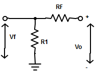 The feedback voltage, Vf = (R1*Vo)/(R1+RF) = (1kΩ*25v)/(1kΩ+10kΩ) = 2.272v ≅ 2.3v.
9. What must be the value of external components used in voltage series feedback amplifier?
a) Less than 1MΩ b) Less than 10MΩ c) Less than 100MΩ d) Less than 0.1MΩ View Answer
Answer: a
Explanation: All external components value should be less than 1MΩ. So, that they do not adversely affect the internal circuitry of the op-amp.
10. Find the block diagram representation of non-inverting amplifier with feedback?
 View Answer
Answer: a
Explanation: The mentioned block diagram is the standard form for representing a system with feedback.
11. Define the input resistance with feedback for voltage series feedback amplifier?
a) RIF = (1-AB) b) RIF = (AB-1) c) RIF = (1+AB) d) None of the mentioned View Answer
Answer: c
Explanation: In feedback amplifier, the input resistance of the op-amp with feedback is (1+AB) times that of without feedback.
12. When the non-inverting input terminal of an op-amp is equal to that of the inverting input terminal (ideally)
a) a–>∞ b) Vid ≅ 0 c) AF = 1+( RF / R1) d) All of the mentioned View Answer
Answer: d
Explanation: When the input at both the terminal are equal, the difference input voltage, Vid=Vin1– Vin2. => Vid≅0 (∵Vin1= Vin2) The open loop voltage gain, A= Vo/ Vid = Vo/0 = ∞ and the closed loop voltage gain, AF= Vo/ Vin = 1+ (RF/ R1)
1. A feedback amplifier is also called as
a) Open loop amplifier b) Closed loop amplifier c) Feedback network amplifier d) Looped network amplifier View Answer
Answer: b
Explanation: A feedback amplifier is sometimes referred as a closed loop amplifier because the feedback forms a closed loop between input and the output.
2. How many types of configuration are available for feedback amplifier?
a) Six b) Four c) Two d) Eight View Answer
Answer: b
Explanation: There are four type of configuration are available. They are voltage series feedback, voltage shunt feedback, Current series feedback and Current shunt feedback.
3. Which of the following is not a feedback configuration?
a) Current-series feedback b) Voltage-shunt feedback c) Current-Voltage feedback c) Current-Shunt feedback View Answer
Answer: c
Explanation: In a feedback amplifier, either current or voltage can be fed back to the input, but both current and voltage cannot be feedback simultaneously.
4. When load current flows into the feedback circuit, the configuration is said to be
a) Current-shunt feedback b) Voltage-shunt feedback c) Voltage-series feedback d) All of the mentioned View Answer
Answer: b
Explanation: In current-series and current-shunt feedback circuit, the load current flows into the feedback circuit.
5. Find the voltage-series feedback amplifier from the given diagram?
 View Answer
Answer: a
Explanation: The mentioned diagram is the voltage-series feedback amplifier because the voltage across load resistor is the input voltage to the feedback circuit.
6. On what criteria does the feedback amplifier are classified?
a) Signal fed back to input b) Signal applied to input c) Signal fed back to output d) None of the mentioned View Answer
Answer: d
Explanation: The feedback amplifiers are classified according to whether the voltage or current is fed back to the input in series or in parallel.
7. The closed loop voltage gain is reciprocal of
a) Voltage gain of op-amp b) Gain of the feedback circuit c) Open loop voltage gain d) None of the mentioned View Answer
Answer: b
Explanation: Comparing the equation of closed loop voltage gain (AF) and the gain of the feedback circuit (B). AF is reciprocal of B => AF = 1+( RF/ R1) ; B= R1/( R1+ RF) => B = 1+( R1/ RF) Therefore, AF = 1/B.
8. Select the specifications that implies the inverting amplifier?
a) V1 = -3v, V2 = -4v b) V1 = -2v, V2 = 3v c) V1 = 5v, V 2 = 15v d) V1 = 0v, V2 = 5v View Answer
Answer: d
Explanation: In inverting amplifier, the input is applied to the inverting terminal and the non-inverting terminal is grounded. So,the input applied to inverting amplifier can be V1 = 0v, V2= 5v
A. Input voltage B. Output Voltage C. Noise D. Voltage Gain b. Only C c. B & D d. A, B, C & D
| |||||||||||||||||||||||||||||||||||||||||||||||||||||||||||||||||||||||||||||||||||||||||||||||||||||||||||||||||||||||||||||||||||||||||||||||||||||||||||||||||||||||||||||||||||||||||||||||||||||||||||||||||||||||||||||||||||||||||||||||||||||||||||||||||||||||||||||||||||||||||||||||||||||||||||||||||||||||||||||||||||||||||||||||||||||||||||||||||||||||||||||||||||||||||||||||||||||||||||||||||||||||||||||||||||||||||||||||||||||||||||||||||||||||||||||||||||||||||||||||||||||||||||||||||||||||||||||||||||||||||||||||||||||||||||||||||||||||||||||||||||||||||||||||||||||||||||||||||
 A at its minimum in the Nyquist plot?
 , Ro = 20 k
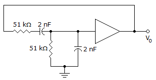
 F, and C2 = 0.002